| Started in: | 2011 |
| Contact person: | Ralf Reulke, Dominik Rueß |
| Staff involved: | Dominik Rueß, Kristian Manthey |
| Detection of large areas of defects in rejected solar wavers. | |
In the solar waver production industry a significant amount of rejected wavers are produced. This is due to pollution of the basis material (e.g. silicon). The company  Greateyes GmbH has developed a camera which is able to record the emission of light, coming from the solar waver, when connected to a power supply. So the process of solar waver principle has been reverted.
Now, the images of this camera can be used to detect darker regions of the waver. These most likely lead to a less efficient conversion to electricity, a lower energy conversion efficiency that is.
A customer of Greateyes GmbH has specialized in exploiting such defect wavers. The waver is cut along borders of defect regions. The resulting, still working parts of the waver can be used for smaller devices like calculators.
The goal of this project was the automated detection of such defect regions. There were 25 sample images. These images came with a variety of unfavorable properties.
The developed algorithm is able to avoid these problems. After detecting the defect regions, finally a clustering is performed. The results are axis-aligned boxes (or "paper patterns") for cutting.
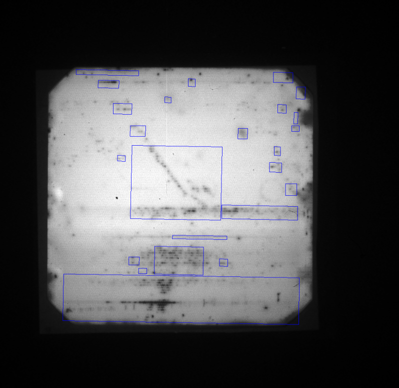 |
| Figure 1: Output of the defect detection algorithm. Small, irrelevant defects are sorted out by a threshold. The axis alignment, with respect to the waver coordinate system, is clearly visible, according to the requirements of the Greateyes GmbH. |


© 2026 - Computer Vision, Department of Computer Science, HU Berlin - - Legal Notice